Explore our industrial-grade components engineered for high-corrosion, extreme thermal, and reactive plasma etching environments.
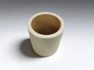
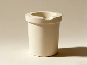
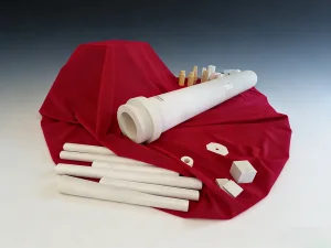
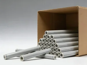
Architectural Sourcing & Material Engineering for High-Yield Semiconductor Sintering, Reactive Ion Etching (RIE), and High-Density Plasma Processing Systems
In modern microfabrication and advanced semiconductor manufacturing, etching equipment represents the foundational pillar governing feature fidelity, yield rates, and atomic-level precision. As integrated circuit (IC) node architectures transition below 3nm, the technological requirements for dry etch process chambers, plasma focus rings, gas distribution showerheads, and wet chemical spray systems have intensified exponentially. Achieving ultra-low particle contamination, high thermal shock resistance, and immunity to reactive fluorinated/chlorinated plasmas requires specialized material science integration.
As an industry-leading Wholesale Etching Equipment Supplier & Factory, our manufacturing ecosystems specialize in synthesizing ultra-high-purity structural ceramic elements—including Yttria-Stabilized Zirconia (YSZ), Silicon Nitride (Si3N4), Silicon Carbide (SiC), Aluminum Titanate, and High-Purity Alumina (Al2O3). By consolidating raw material formulation, cold isostatic pressing (CIP), vacuum sintering, and sub-micron 5-axis CNC diamond grinding under one roof, we provide enterprise fabs and equipment builders with unprecedented structural reliability and thermal stamina.
Comprehensive comparative performance metrics evaluating ceramic substrates under aggressive halogen plasma and chemical bath environments.
| Material Matrix | Density (g/cm³) | Flexural Strength (MPa) | Thermal Conductivity (W/m·K) | Plasma Resistance Index | Primary Etching System Application |
|---|---|---|---|---|---|
| Yttria-Stabilized Zirconia (YSZ) | 6.05 | 1100 - 1300 | 2.7 - 3.0 | Ultra-High (Fluorine/Chlorine) | Plasma Focus Rings, Precision Nozzles, Wafer Chuck Inserts |
| Magnesium-Stabilized Zirconia | 5.74 | 750 - 900 | 2.5 | High Thermal Shock | High-Temperature Vapor Etch Liners & Insulation Shields |
| Silicon Nitride (Si3N4) | 3.25 | 850 - 1000 | 30 - 85 | Exceptional Erosion Resistance | ICP Plasma Chamber Walls, Structural Fasteners, Pumps |
| Aluminium Titanate (Al2TiO5) | 3.55 | 40 - 70 | 1.5 - 2.0 | Thermal Shock Impervious | Low-Expansion Chemical Etching Tanks & Molten Metal Fittings |
| High-Purity Alumina (99.99% Al2O3) | 3.96 | 380 - 450 | 32 | Moderate Plasma / High Chemical | Gas Distribution Plates, Wet Etch Chemical Manifolds |
Strategic, operational, and material advantages derived from Yixing's world-class advanced ceramic industrial ecosystem.
Unlike regional assemblers, our China factory spans the complete production lifecycle: from high-purity chemical powder synthesis (YSZ, Mg-SZ, AlN) to green body shaping, high-temperature sintering in vacuum furnaces, and precision CNC diamond grinding. This vertical integration drastically reduces lead times and removes middleman markups.
Capitalizing on China's massive industrial infrastructure and standardized quality protocols, we offer OEM and ODM etching equipment components at unmatched unit-cost economics. Fabs can lower Total Cost of Ownership (TCO) while achieving equivalent or superior component life cycles compared to legacy Western suppliers.
Every piece of etching equipment structural ceramic undergoes 100% non-destructive testing (NDT), coordinate measuring machine (CMM) dimensional verification, and optical particle cleanroom inspection. We guarantee zero lattice defects, micro-crack elimination, and extreme tolerance control up to ±0.002mm.
Deploying advanced ceramic technology across high-value semiconductor microfabrication, PCB chemical etching, and clean energy sectors.
In Reactive Ion Etching (RIE) and Inductively Coupled Plasma (ICP) systems, plasma sheath erosion rapidly degrades metallic components. Our high-density Yttria Stabilized Zirconia focus rings and Silicon Nitride liner shields withstand aggressive CF4, C4F8, and SF6 gas discharges, preventing micro-particle contamination during wafer patterning.
Printed circuit board wet etching lines utilize concentrated ferric chloride (FeCl3) and cupric chloride (CuCl2) chemical sprays. Our acid-proof Aluminium Titanate nozzles and high-purity Alumina valve manifolds ensure chemical inertness, eliminating nozzle swelling, wear, and flow disruption.
Photovoltaic silicon wafer manufacturing requires isotropic etching and surface texturing using nitric and hydrofluoric acid blends. Our ceramic engineering solutions provide chemical resistance against strong oxidizing acids, maintaining process bath purity and maximizing solar cell efficiency conversion.
From titanium alloy orthopedic implant micro-texturing to aerospace turbine blade chemical milling, ceramic structural components deliver the mechanical stiffness and thermal stability required during high-stress chemical processing environments.
Pioneering high-entropy ceramic compounds and next-generation atomic layer processing solutions.
As semiconductor nodes shrink to 2nm and beyond, traditional plasma etch methods cause unacceptable lattice distortion. Atomic Layer Etching (ALE) removes material layer-by-atomic-layer. ALE equipment demands specialized Yttria (Y2O3) and Zirconia ceramic components with near-zero sputtering yield to ensure process repeatability.
The rapid adoption of wide-bandgap semiconductors for EV power electronics and 5G telecommunications requires high-power ICP-RIE etching equipment. Ceramic components within these chambers must endure extreme thermal density without outgassing or structural degradation.
To extend the lifespan of consumable chamber parts, our R&D hub is pioneering multi-component ceramic compositions (such as AlN-SiC composites and magnesium-yttria co-stabilized zirconia), offering up to 3x longer service life under fluorine-rich plasma bombardment.
A Premier Pioneer in High-Performance Advanced Ceramic Manufacturing & Integrated Etching Equipment Solutions Since 2003.
Founded in 2003, Yixing Qiangguang Ceramic Materials Co., Ltd. is a professional provider dedicated to the research and development (R&D), manufacturing, and application solutions of high-performance advanced ceramic materials. It is among the few enterprises in China that possess a complete industrial chain, covering key links from powder forming, sintering and precision machining to the provision of integrated application solutions.
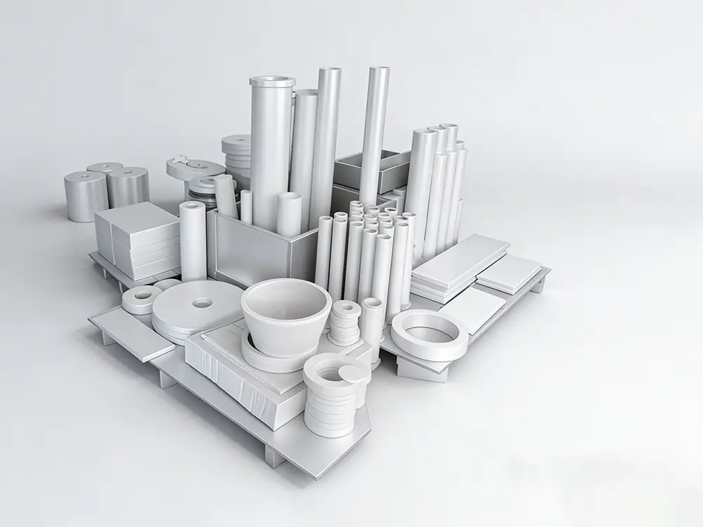
The company is also a rare domestic manufacturer engaged in the R&D, production, and supply of a comprehensive portfolio of ceramic materials. Its product range covers zirconia, yttria, alumina, magnesia, aluminum nitride, boron nitride, silicon nitride, silicon carbide, aluminum titanate and other key ceramic materials for industrial use.
Benefiting from excellent product performance and stable quality, its products are extensively utilized in various high-end fields, such as food and medical industries, new energy vehicles, laser semiconductors, petrochemical engineering, powder metallurgy, national defense and military, as well as aerospace sectors.
Adhering to the core principle of "creating value for customers", Qiangguang provides customized and cost-efficient advanced ceramic solutions tailored to the specific demands of different customers. It is supported by high-quality after-sales services and a strict full-process tracking system, which effectively enhances cooperation efficiency and promotes continuous quality improvement.
At present, the company's products are sold well across the country and exported to Italy, the United Kingdom, Australia, Japan, Malaysia, Thailand, Hungary and other countries and regions. Committed to delivering high-quality products at reasonable prices, Qiangguang sincerely looks forward to establishing long-term and stable cooperative relations with global partners.
Streamlined 5-step strategic procurement protocol designed for semiconductor tool manufacturers and tier-1 fab suppliers.
Our engineering team reviews your 2D/3D component schematics, evaluating thermal expansion coefficients, plasma exposure conditions, and mechanical load limits. Finite Element Analysis (FEA) is conducted to optimize geometry.
Depending on your chemical environment (e.g., HF wet etch vs. Cl2 dry plasma), we select the optimal ceramic substrate (Yttria Zirconia, Mg-Stabilized Zirconia, Silicon Nitride, or High-Purity Alumina) to balance lifecycle and procurement cost.
Green body components are formed using Cold Isostatic Pressing (CIP) up to 200MPa, followed by high-temperature vacuum sintering in high-purity atmosphere furnaces to achieve near-theoretical micro-density.
Using ultra-precision 5-axis CNC diamond grinding centers, components are machined to sub-micron tolerances (±0.002mm), with surface polishing achieving mirror-like Ra < 0.02 µm finish for cleanroom integration.
Expert insights regarding advanced ceramics, etching equipment sourcing, material performance, and factory customization.
Comprehensive product catalog supporting semiconductor processing, precision grinding media, and structural thermal barrier solutions.